Two-Photon Polymerization
Materials and techniques for 3D fabrication
From Optical Tweezers to Asymmetric Beads, explore the potentiality of 2pp
From Optical Tweezers to Asymmetric Beads, explore the potentiality of 2pp

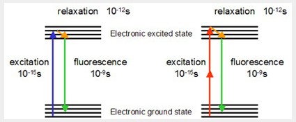
Two-photon induced photopolymerization is widely used in areas such as optics, biology and electronics due to the reproducible sub 100nm resolution, 3D processing and maskless lithography. This technique consists into focusing a pulsed laser beam into a photopolymer through an objective lens, leading to the multiphoton absorption only at the focal volume without affecting the outer resin (Figure 1)

The simultaneous absorption of two-photons creates radicals in the photo-initiator, which triggers the monomer for cross-linking. Thereby, moving the sample in 3D with respect to the beam or vice-verse allows the fabrication of the 3D micro-nano structures.
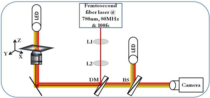
Many experimental setup for two photon lithography (TPL) rely on a Ti:sapphire system, thanks to its high repetition rate and broad wavelength tuning to excite most of the monomers and photoinitiators. However fixed wavelength alternatives such as a mode-locked Er- doped fiber laser lasing at 780nm can be userd for many resins. An example of experimental setup with the latter laser is shown in Figure 2.

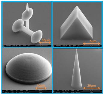
When mixed with the monomer and exposed to the laser beam through a low or high NA objective, the photo-initiator starts the polymerization with a minimum threshold power. Increasing the optical power by a few milliwatts amount, the polymerized structures achieve a good 3D mechanical stability, even with only the external surface exposed. The material is then developed with a few seconds of rinse in methanol and Isopropanol. The developed structures are then exposed with UV to complete the polymerization of the resin inside the inner volume(Figure 3).

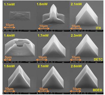
Structures such as micro-prisms, micro-lens, micro-cones and asymmetric beads can be fabricated with a single shell exposure, demonstrating the versatility and reliability of the material in term of geometrical shape and curvature. In Figure 4 we show examples of structures fabricated with increasing amount of power and different photoinitiators. The monomer used is an acrylic BPA-EDA.

We can see that BDEB has a higher cross linking threshold respect to ITX, but the latter needs a higher power to withstand the structures with just a single-shell exposure.