Plasmonic Hole Arrays
Substrate for neuron growth and synapse excitation
Design and Fabrication of the nanobio tool for single-molecule activation
Design and Fabrication of the nanobio tool for single-molecule activation
The plasmonic Hole Array represents a suitable substrate for neuronal growth and synapses excitation. This device has been designed for FOCUS, a European project whose goal was to develop molecular devices for single molecule detection and activation.
The concept behind the plasmonic hole array is the focusing of incoming light down to the size of a molecule,that is around 10 nm. To overcome the limitation of classic optics, we rely on the interesting properties of plasmon polaritons. Under some conditions, the light incident on a substrate trasnforms into an electronic wave that can travel along a metal-dielectric interface and can thus re-transform into light at the end of the path. With a 2D holes array made of 10 nm holes we can thus "focus" the light to that dimension, providing a near-field illumination on the holes. So, if we grow neurons on the substrate, we can excite single synapses.
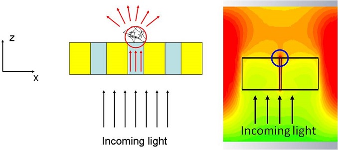
The device we have explored is formed by an array of sub-wavelength holes drilled in a metallic (gold) slab. The working principle assumes a plane wave-like source illuminating the device that performs a kind of filtering by allowing the passage of light only through the holes. Each hole has a constant diameter which is ranging from 20 to 1000 nm, while the light source has a wavelength of 514/530 nm and the inter-hole distance is 1 µm.
Obviously, in order to reduce the focal spot as much as possible, 20 nm holes are preferable over higher values. However, the numerical simulations have to take into account also the fabrication constraints which set the holes diameter limit at 80 nm.
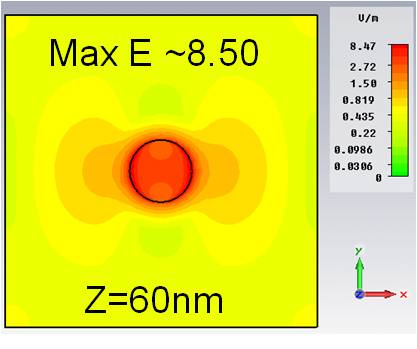
The figure shows the electric field distribution on a gold-substrate when a hole of 200 nm is drilled in it. The source is chosen as a plane wave at 530 nm with polarization along x-axis and normal incidence. The field source is 1 V/m. The maximum field value is found at 8.5 V/m with signal-to-noise ratio around 23 in x-direction and 4 in y-direction. Similarly, the figure below shows the electric field when the diameter of the holes is 80 nm and the thickness of the slab 100 nm.
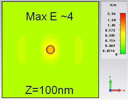
The maximum electric field value is found around 4.0 V/m, lower than in the previous case. However, the two quantities we are interested in are the focus spot (now around 40 x 40 x π nm2) and the signal-to-noise ratio which is, for the present case, about 25 along x-direction and 8 along y-direction. Both these parameters are significantly improved when moving from one figure to the other (we recall that Raman spectroscopy is proportional to the fourth power of the electric field, namely little difference in the electric field can easily be big difference in terms of Raman signal). Finally, we show the electric field profile along a line passing through the holes along x-direction (thickness 100 nm, holes diameter 80 nm).
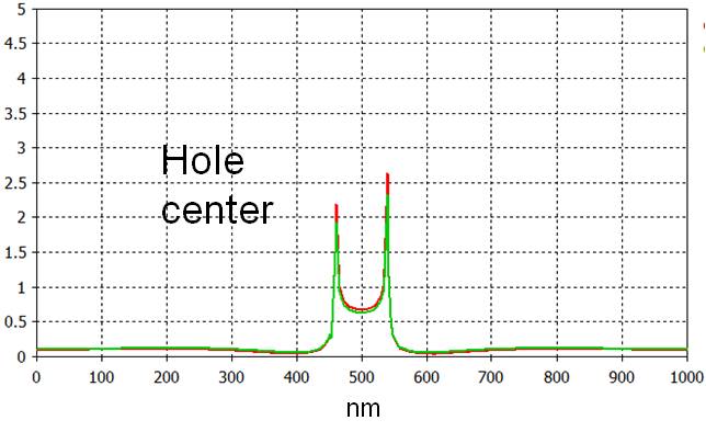
The plot gives maxima of the electric field at the edges of the hole, which can be explained in terms of SPP. In fact, the light source couples with one side of the slab, here it excites SPP which propagate along the walls of the holes. We can neglect periodicity contributes ought to the high period of 1 µm. Hence, we have seen that decreasing the holes diameter and increasing the slab thickness plays a favorable role in terms of light spot and signal-to-noise ratio. Up to now, the best signal-to-noise ratio was 25-x and 8-y with in-plane spatial localization of 40 x 40 x π nm2.
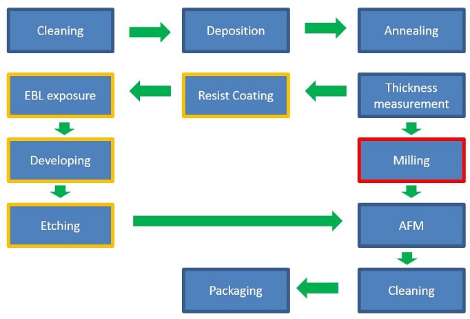
2D Plasmonic holes arrays have been fabricated on borosilicate substrate. The fabrication process is outlined below.
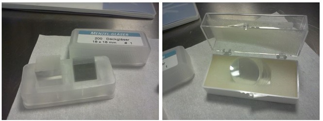
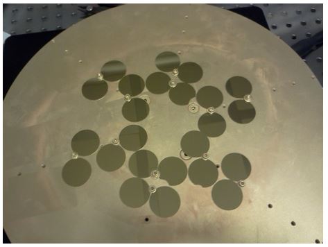
The base substrate is a coverglass, that is a square glass 18x18 mm2 or round glass 25 mm diameter with a thickness of approximately 160 µm.
The substrates must be cleaned of impurities. So at first we use the following process:
Put the substrates in a beaker with acetone.
Put the beaker in a ultrasonic tank and clean for 5 minuites.
Put the substrates in a beaker with isopropanol.
Rinse the samples in demineralized water.
Dry the substrates with N2 compressor.
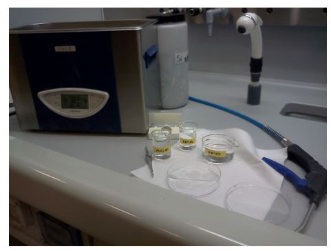
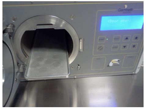
It is suggested to put the glasses in a Plasma system. 5 minutes under oxigne plasma at 55 W will be sufficient to remove any biological contamination.
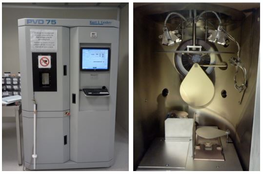
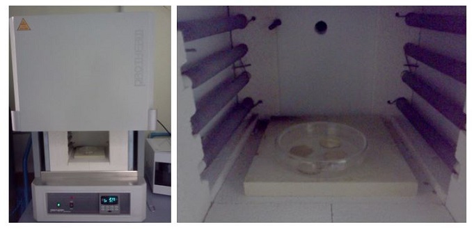
In order to increase the stability of the structure and to smoothen the gold surface, we heat the substrate in the same vacuum chamber of the evaporator. We set a plateau at 350°C for 2 hours, with a ramp of 3°C per minute.
In alternative to the evaporator heating, we can have annealing in a furnace. In this case the optimised parameters are a set point of 500°C for 4 hours and a ramp of 3°C per minute.
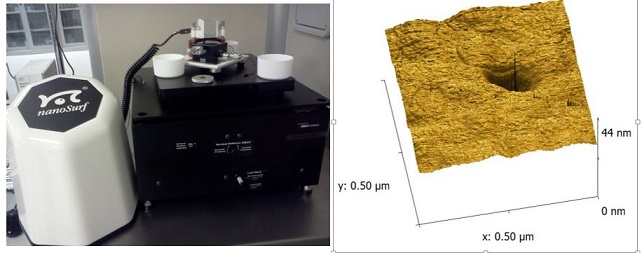
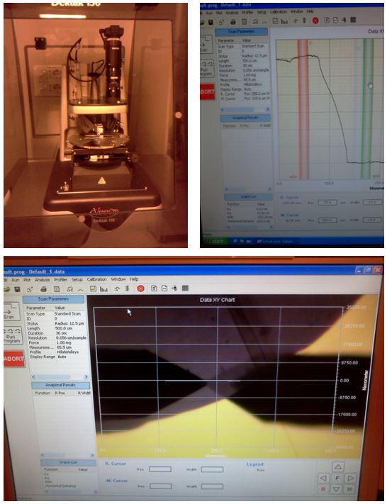
To be sure that the amount of gold deposited is exactly 60 nm, we use a profilomter. After scratching one of the sample, we measure a scan of 100 µm at 0.006 µm resolution, hills and valleys profile.
Now that we have the golden substrates, we have two approaches to obtain the plasmonic holes. One way is to use the electron beam lithography, the other is to use focused ion beam.
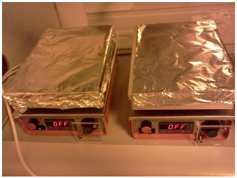
In this case we have to prepare the substrate for the exposure. So we have to spin photoresist on it. A layer of 150 nm of 950 PMMA A2 would be sufficient, so we spin at 1000 rpm for 90 seconds.
The PMMA is hardened with hot plates, putting the samples at a temperature of 180°C for 90 seconds.
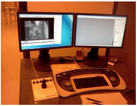
The samples are then inserted in the EBL chamber.
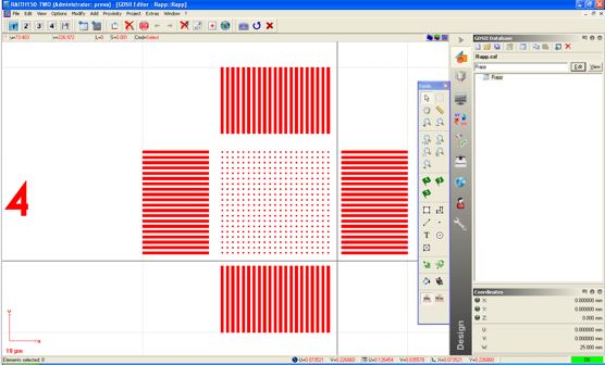
Here, a pattern with an array of holes is exposed on the PMMA. For reference, a set of lines are added to the pattern.
After the exposure, the PMMA is developed with a rinse in IBMK/IPA for 30 seconds,then in isopropanol for 30 seconds and dried with N2. The developer will open windows on the gold. At this point we have to remove the gold not covered by PMMA. We have two approaches: dry or wet etching. For dry etching we can use the Reactive Ion Etching (RIE). For the wet, we can rinse the sample in gold etchant.

After we have removed the patterned gold, we remove the remaining PMMA rinsing the sample in Acetone.
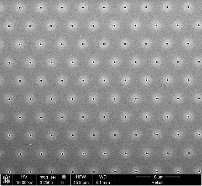
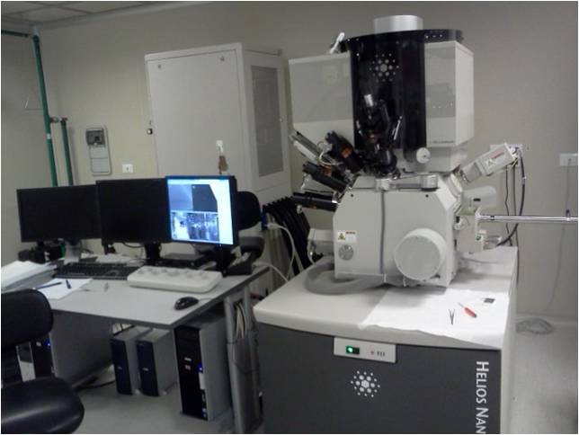
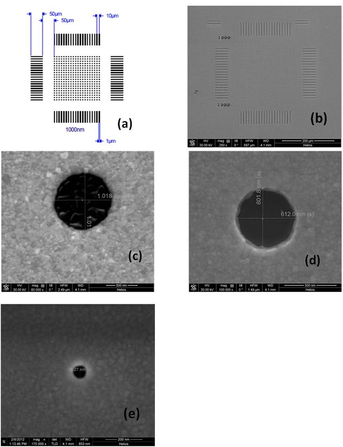
In alternative the sample can be milled with a Gallium ion beam (Helios Nanolab 650 FEI) at 30 KeV and 0,69nA, defining a 20x20 matrix of holes with 20 rectangular markers 50 x 1 µm2 on each side.
Different geometries have been implemented on the holes grid, varying from 1000 nm to 80 nm, in order to test their plasmonic properties.
The sample topography has been characterized recurring atomic force microscopy, using the nanoAFM in tapping mode, with a high aspect ratio tip.