Nanoantennas
From plasmonic excitation to super light absorber
How to Fabricate nanoantennas
How to Fabricate nanoantennas
Nanoantennas have been heavily used for plasmonic excitation and to enhance Raman spectroscopy. Recently there is an increasing research in the fabrication of low-cost super absorber for heating applications like solar cells. The goal is to catch all of the light hitting a surface, with barely no reflection at all. It is known that nanoantennas have an absorption spectrum dependent on their geometry. So, by shaping them accurately, it is possible to provide a surface that absorbs every wavelenght incident on them, provided that these antennas are close enough. Following i'll show the procedure to fabricate nanoantennas on membrane
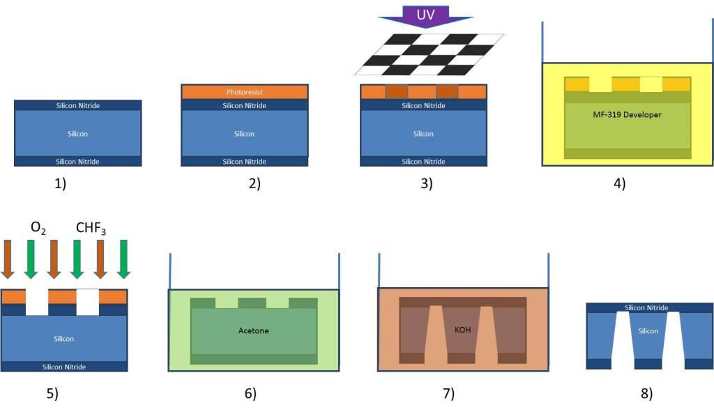
The membrane is obtained from a wafer Si3N4 - Si - Si3N4 wafer. The silicon has a thickness of 500 µm while the nitride can be 100 or 200 nm. Spin one of the nitride faces with S1813 at 4000 rpm and bake it at 90°C for 3 minutes. The layer thickness will be approximately 1.5 µm. Apply a mask lithography with the windows for the membranes. The exposure can be either soft or hard contact (no need for extra precision) for 15 seconds, after that develop with MF-319 for 1 minute. Rinse in water and bake the wafer for 1 minute to dry it completely. The developer will expose windows of nitride. To remove the Si3N4 exposed, we use a Reactive Ion Etching (RIE) procedure. We use CHF3 (sccm 70) and O2 (sccm 5). The pressure will be 5 Pa (maybe) and the RF power around 70 W. After 2 minutes of process, the Si3N4 exposed is removed. In case of a thicker layer of SiN (like 200 nm), the RIE recipe should be prolonged, but this could remove the whole resist layer. In this case, it’s better to use different parameters, like a lower RF power (25 W) and less Oxygen. Remove the residual resist with Acetone, better to rinse it in a ultrasonic tank. It could be useful to clean the wafer with a tissue imbued with acetone, in order to clean it very well. Better to clean the back of the wafer too. It is very important to clean well at this point, since everything will be more delicate after the etching. Put the wafer in a solution with 100 g of KOH and 150 ml of H20. Heat the solution on a hot plate at 105°C. The acid will etch only the silicon with an etching angle of approximately 54°. It is better to put the wafer with the exposed part towards the top of the flask. To avoid contact with the bottom, you can use a proper support. The acid will etch the silicon in 6-9 hours. Don’t forget to put some lid on top of the beaker (another larger beaker or some film), otherwise the water will evaporate. After that, rinse the wafer in milliQ water. The wafer is ready. In order to separate the single membranes, be extra cautious and consider the silicon crystal structure.
The sputtering consists in bombarding a metal target with an accelerated plasma of gas. The particles scattered by the ions drop on the substrate underneath, covering it with high uniformity.
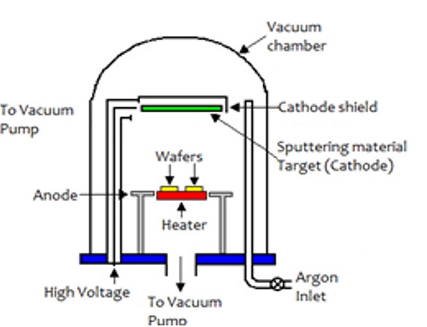
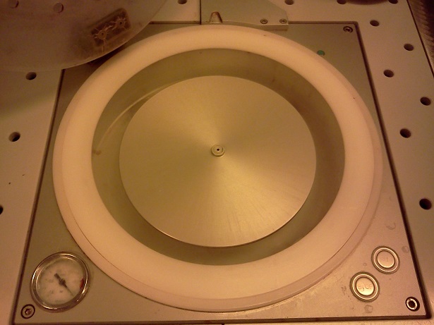
There are different kind of sputtering machine, with one or more metal targets and with the target on the top or the bottom. The one I used the most is a Quorum Q150T ES. Following is the standard procedure to use it.
Open the Argon gas valve. The Argon is the gas used to strike the metal target
Open the Nitrogen gas valve. Nitrogen is used to vent the chamber
If not done already, open the chamber with the selection of QT vent Chamber, then hit Run. This way the pump stops and the Nitrogen enters the chanmber
Check the O-ring and clean it from dust
Inside the chamber there is a weight monitor that controls the quantity of the material sputtered. Be careful not to touch it unless you have to substitute it. Extract the plate.
Check if the correct target has been inserted. Otherwise access the back of the target by removing the lid. Remove the electrodes from the back of the target, turn the safety screws and extract the target with its cathode. Remove the armor that push the target against the cathode and remove the target. Substitute the target with the one needed. Remount everything.

At this point there are two ways to sputter. One is the standard way, where the sample is put on the plate and sputtered from the top. Another way is the spiedo modality, where the sample is mounted at an angle and rotated, to grant a deposition on the whole sample. We start seeing the first one.
Put the sample on the plate, the face that has to be covered should be up. It is recommended to insert a piece of clean silicon between the sample and the plate, to reduce contamination of the sample and to help the removal after sputtering. In case the insertion of the plate back in position is difficult, it is possible to remove the chamber, put the plate and reinsert the chamber. In this case pay attention to reposition correctly the chamber to avoid vacuum losses.
Close the chamber and select the desired program. Check the parameters with Edit profile menu to deposit the correct amount of metal. It is possible to decide either the depositon time or the amount of nanometers. The latter depends on the sputtering current and the Tooling factor. In this example, related to the Antenna fabrication , I select a deposition of 20 nm of copper.
Hit Run the process. The Nitrogen valve will close and the pump will start. When high vacuum is reached, the Argon will flow inside and, after some seconds for saturation, the gas will be ionized. The plasma will bombard the target and particles will drop on the sample and on the scale inside the chamber.
When the scale detects the amount of nm set in the process or after the set amount of deposition time has passed, the pump stops and the Nitrogen enters the chamber.
Open the chamber and retrieve the sample. Otherwise change the target and/or the process and repeat the procedure.
When the sample is ready, remove it from the chamber and select the process QT Vacuum Shutdown to keep the chamber closed and avoid contamination.
Compile the machine report and close the Argon valve

This procedure requires the substitution of the chamber with one with a lateral access. Then you mount the sample on a tilted stub, usually with an angle of 45°. The stub is inserted at the end of a thin rod. The rod ha to be inserted in the lateral aperture of the chamber, from inside. then the rod can be rotated to the desired angle, to make the sample face the metal target. At this point we close the chamber and we proceed with the standard way, editing the process and running it. But during the sputtering, we rotate the rod from the external handle of the chamber,so that the metal will cover the sample at 360°. Of course in this case the amount of nm set will be different respect to the one set in the standard depositon. In the latter case, in fact, the amount set will be dsposited on the required face. In the other case, instead, because of the rotation, only a fraction of the metal will cover the area of the sample, so a higher amount of material has to be set.

Check always the parameters before the sputtering and, if possible, put the samples always in the same position. In fact the sputtering process is not perfectly homogeneus, the central part of the chamber receive more sputtered material respect to the outer partand also a higher quota will influence the deposited amount (higher quote, more material on the center, less in the extremeties). Also consider that the Tooling factor, that is the conversion between the amount of material deposited on the scale and the one that really ends on the sample, may vary a little after time, since the scale becomes dirtier. Also the sputtering current influences the quality of the sputtering. Higher currents make the sputtering rougher, lower current grants smoother profiles. However, for important samples, check the real depsosition under a profilometer.
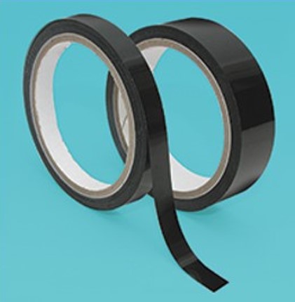
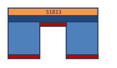
Now that i have a membrane with a face covered with 20 nm of Cu, i require an optical mask. Usually the mask is applied to a photopolimer, that is something that will cover and protect the sample underneath a part from the exposed parts. I use the resist S1813. It is important to take some amount from the main bottle, store into a personal flask and put the name and the date of first use, to dispose it properly when expired. Expiring is not only related to age, but also to dirtiness, evaporation and exposure to light. It's best to change after a few months. Also, it is needed to write on a label the dilution. The resist usually has to baked after the deposition, so i turn on the hot plates to the desired temperature before spinning. For S1813 the temperature is set around 90°, but it varies for different photoresists. At this point i prepare the sample. Unless the sample is sturdy like a piece of silicon, it's a good idea to attach it to a bulky material, like of course a piece of clean silicon. I have to cover in polymer the face that has not been previously metalized in copper. Since my membranes are quite small and very fragile, I prepare a little piece of silicon with two carbon tape stripes on top. I put my sample in the middle of the carbon strips, so that the membrane doesn't touch the adhesive but is close enough to the substrate to avoid (partially) that the resin goes underneath during the spin. In our clean room we have 2 types of grafite tape. The first one is the model 77817-20, yellow label, very adhesive and deformable, it can be used multiple times but easily leaves residues. The secon is the carbon tape 16084-7, white label, less adhesive and more rigid, leaves less dirt but is less friendly. For the membranes, the second one is more suitable since the sample is fragile and i need to remove with ease.
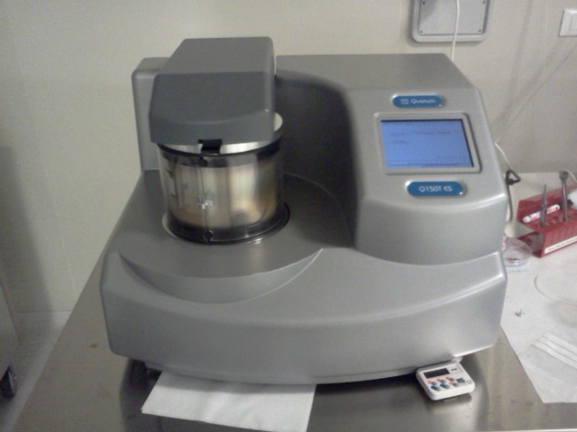
The spin machine I used is a model Sawatec SM-180. It is similar to a cotton candy machine, with a central chamber in which a rotating disk is postioned. The disks have a central bulge that can vary in dimension. This crossed protrusion is connected to the vacuum system of the machine; during the spinning operation it "sucks" the sample to keep it in the center of the chamber. It is important to select one with the dimension close to the sample (but slightly smaller) or use a substrate big enough to cover the entire cross. This will grant a good adhesion and avoid to make the resist enter inside the vacuum system. So, once inserted or substituted the plate, i put my sample on top. Depending on the machine, there could be the possibility to test the vacuum before activating the spin. If so, i press Vacuum on and check if the sample doesn't slide.
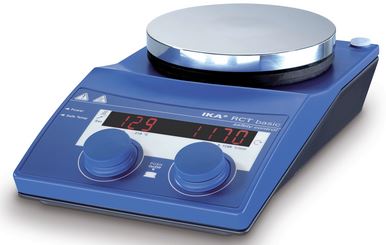
By this time, the hot plate should be at the right temperature (90°). We use a model IKA RET, PBInternational. For this case, it is important to use a tempertuare lower or similar to the one for resist transition, to avoid an eccessive hardening and so a more difficult removal. Instead, if we need to do some lithography, it is good to heat well, crystalizing the resist. The resist hardening, in fact, depends by the temperature, light exposure and time duration. For my sample, i heat for 3 minutes, than i remove it from the hot plate. We should be ready for the electron microscope.
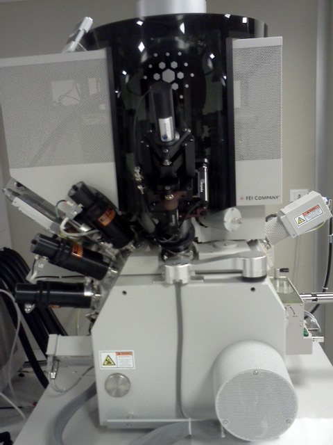
The fabrication of the protruding antennas will be done via dual beam system. The model I used is a Helios NanoLab 650 from FEI company, controlled by the software XT Microscope Control.
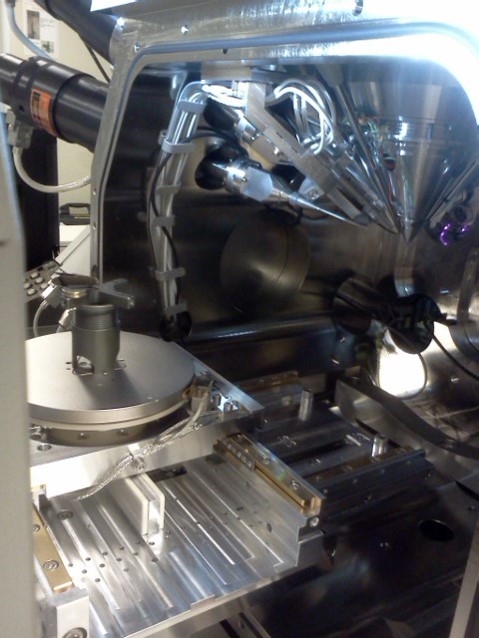
Once the camera has reached a sufficient vacuum level, the electron beam can be switched on with Beam on command. Since the sample has resist on it, it is mandatory to scan it the least possible to avoid hardening it. So we focus at the beginning on an impurity outside of the sample to correct the focus. Then we give the machine a reference by linking the distance sample-to-column to the focus. In this way the machine will give the exact distance between the sample and the electron column if the focus is well done. Since it is a critical value, it is mandatory to repeat from time to time. Once linked, i focus again on the external part of the sample, far from the membrane and i link again. Then I move the sample to a distance of 4.1 mm from the column. This distance is the optimal one for operating with this SEM model. At this point i tilt the sample at 52°, to have it perpendicular to the FIB column. I turn on the FIB filament. If the linking has been made correctly, both SEM and FIB column will look at the same spot. I correct the focus on both the columns as best I can. Since the FIB vision can easily remove the metal from the sample, it's better to have a reduced window of scanning or to do first a few holes with the Spot command and then correcting the focus and aberration looking at the border of the hole. When i'm satisfied, i can make a hole in the angle of the membrane and check the borders. if they're fine, i can move on, otherwise i keep correcting.
Time for the patterning. I need to create antennas in the polimer underneath the Si3N4 membrane. So i should dig round holes with the FIB. I choose a square pattern with a pitch of 1 µm to have a dense array of antennas. The column parameters will be V=30 KV, I=40 pA, dwell=200 μs, z=10 μm. It's important to zoom so that the pattern is the biggest possible to increase the resolution. Also, in case of small holes, is better not to watch the sample after the milling otherwise some particles could be scattered inside the holes. During milling, i watch the speciment current to monitor the depth of the holes. In fact at the beginning the current will have a certain value, due to the ions that travel from the sample metal to the detector. Then, while the FIB destroys the metal, the current will lower. In the end, when the FIB makes a through hole in the smaple, the current will rise again and i can stop the milling.
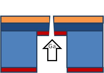
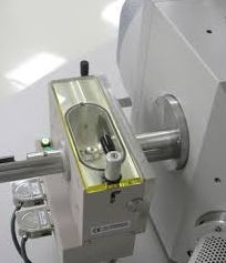
After some arrays of holes i can Vent the chamber and observe my sample with a microscope. I use the Nikon Eclipse LV100 to observe the through holes. The SEM cannot see them since it will expose the resist. It is important to watch the structures with the yellow filter NCB11 to lower the photoresist exposure. If the holes are there, i can cover with gold.
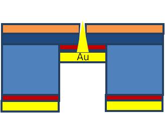
To create the antennas, i need to cover the lateral surfaces of the holes with gold. So i insert the sample in the sputtering, change the target from copper to gold and deposit 50 nm of gold. It's important to put the samples always in the same position. Also i put an additional silicon piece for testing.
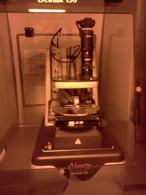
Is it really 50 nm? Now this parameter is important, since i must be sure that the sample is reproducible. So i take the silicon piece I put in the sputtering, scratch it a little with the tweezers and bring it under the profilometer Veeco Dektat 150. Its software is quite intuitive. First i touch the icon with a reverse flag to lower the tip of the profilometer down to the sample. The tip will touch the sample and then it will go up 1 mm. Now with the micromanipulator i move the sample to approach the scratch to the tip. I set the scan time, the lenght and the force of contact (2 mg for the gold is ok). I also set the tip dimension, that is the scan resolution. In my case 12.5 µm is little enough. I launch the scan and the tip will touch the sample, moving along the vertical direction and following the profile. To have a better meaure is important to start and end the scan on the gold part, putting the scratch in the middle. At the end i will know the exact amount of gold sputtered.
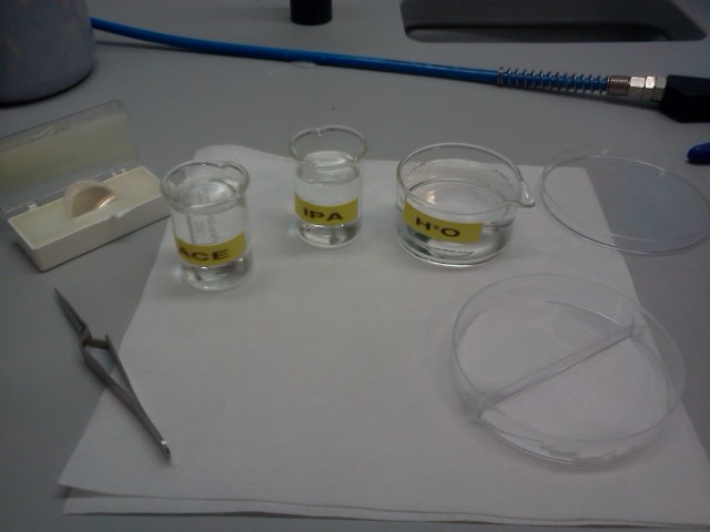
The unexposed resist has to be removed. So with utmost care we put the sample in a beaker filled with acetone. To quicken the process, the Acetone can be heated to 45° with a hot plate. After the Acetone we insert the sample in IPA to leave the residues. The resist will go away leaving only the golden antennas.
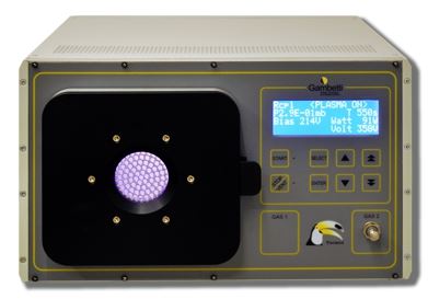
In order to shrink the antenna a little bit, improving also their roughness quality, we put the membrane in the O2 plasma, setting 100% gas, 100W of power and 120 seconds of exposure.
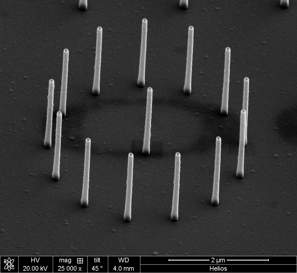
I sputter 20 nm of gold on top of the antennas before seeing them again with the SEM. If everything is done well, this is the result
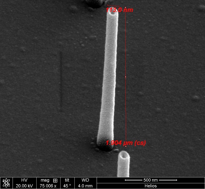
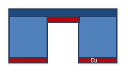
We take a membrane and we deposit 20 nm of Cu on the back, paying attention not to put the membrane in direct contact with the chamber. To help us , we can use additional substrate with a hole in the middle or with lateral steps. The recipe is “copper”; we should edit to set the correct thickness and ignore the message of warning. After the sputtering, we can spin a layer of S1813 on the membrane. Again we need a special support, since we have to keep the membrane a bit distant from the support. A solution is provided by a microscope glass with paper glued on the upper face and two lateral bands made of carbon tape. The carbon tape can keep the membrane in position and a bit suspended, while the paper can absorb the spinned resist preventing it from going under the membrane. The recipe used is PMMA 2500 to obtain a layer of more or less 2 μm. Then we put the membrane on a hot plate at 90°C for 3 minutes. Now the membrane is ready for the FIB milling, I insert the membrane with the back exposed (the Cu face) paying attention to keep the membrane suspended on the stub. The parameters used for the creation of needle are: V=30 KV, I=40 pA, dwell=200 μs, z=10 μm. The pattern will be a rectangle with the pitch indicating the distance between the needles. In this case we use a pitch of 2 μm. With this pitch we will not need particular attention when we will remove the resist (just acetone and N2). Instead, if we keep the distance smaller, the antenna could collapse towards each other, so will be needed a washing in liquid oxide after acetone. So, we search for the membrane, we focus on one angle, we tilt at 52°, we correct the astigmatism and focus of both the column, making also a few holes to check the parameters and we can start. The important thing is, after the focusing, to use the least possible the electron column. In fact, since the membrane is not very thick, the electrons can travel through the nitride and hit the resist on the other side, thus exposing it, and the antenna will not be exploited. So we have to move and observe with the ion beam. When we think we did our best, we remove the sample from the SEM and we develop it. The developing is made by rinsing the membrane in acetone until we see that the resist is removed and then blowing N2 to dry it. The needle should be now created, we can observe them directly at the optical microscope. In order to shrink the antenna a little bit, improving also their roughness quality, we put the membrane in the O2 plasma, setting 100% gas, 100W of power and 120 seconds of exposure. Finally, to be seen at the SEM again, I sputter 20 nm of gold on top of the antennas. If the result is good I’m happy. One important thing. If we want to use the membrane again, a good idea should be to remove the gold layer before the spinning, otherwise the parameters for the ion column will change. So a gold etching before starting again is mandatory. The antennas shouldn’t be influenced by the etching.