Plasmonic Cantilever
Combine plasmonic nanocone with photonic crystal
An effective technique to achieve single molecule activation
An effective technique to achieve single molecule activation

AFM cantilever are widely used for profilometry as seen in the AFM section. However they are needed also in experiments involving molecule activation and pulling. The idea is to build a nanocone on the tip of a cantilever and enhance the plasmon polariton coupling by means of a photonic crystal cavity built around the cone.
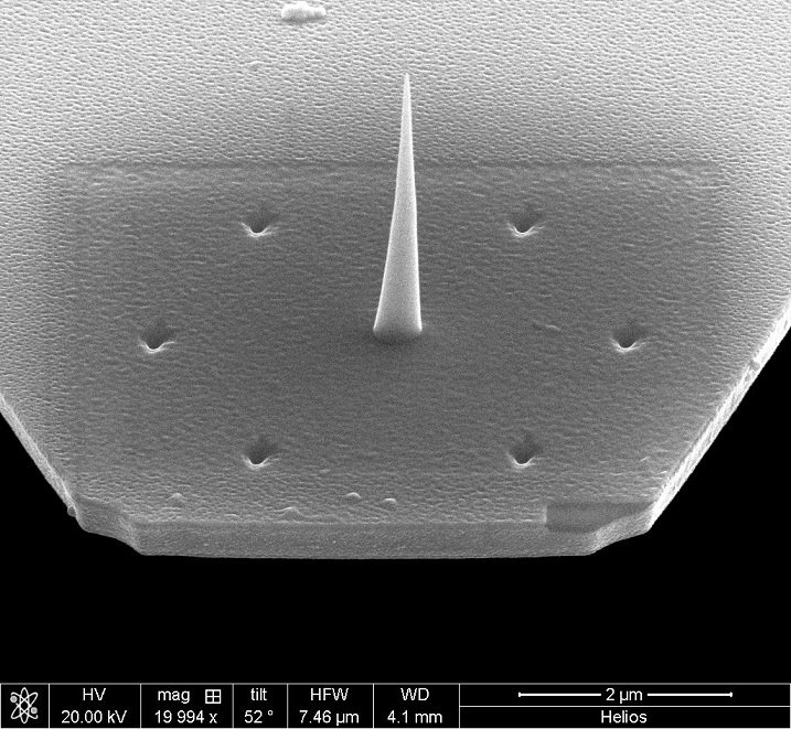
The cantilever I'm going to use is shown in the following picture.
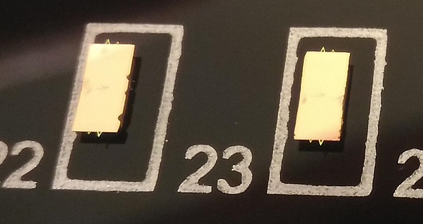
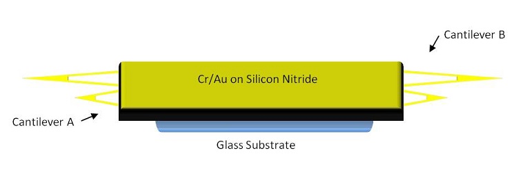
Each chip has two cantilevers for side, one bigger than the other. We are interested in the longer cantilever, that is the softer since we will use it on biological sample. The softness is due to the fact that it protrudes more from the chip. We work on just one of the two cantilevers B. The first important thing is that the cantilevers are extremely fragile. Little shocks can detach them, so we must be very careful in all the processes.
So, first thing we prepare the stub for the evaporation exposure. We take a SEM stub with a string of carbon tape, the more rigid, and we remove some of the adhesion power by putting fingers on it. In fact it is very important that the carbon tape is strong enough to keep the sample in position and be conductive, but mild enough to change the position of the chips when required without exerting too much force (and shock). Then we remove one chip from the box and we put it on the carbon tape. A good choice for this is to use the curved tweezers. We put the chip on the carbon tape letting the glass part adhere to the tape, then, forcing slightly on the sides, we detach the chip and we attach on the carbon tape by the lateral surface.

We bring the stub to the sputter machine, using the spiedo modality, having the faces of the chips inclined 45° circa respect to the gold target. This way the gold can be deposited on the whole cantilever without shadows. We set a thickness of 30 nm in spiedo. Paying attention to the thickness monitor, we let the sputter deposit 15 nm of gold, then we rotate by 180° the rod (during the sputtering process) to cover the opposite side of the chips. At the end we have the cantilevers covered with 15 nm of gold on each side. After the sputtering, with care, we rotate the chip to let it adhere flat on the carbon tape, with the glass adherent. We insert the stub in the SEM and we prepare the pattern of the photonic crystal cavity.

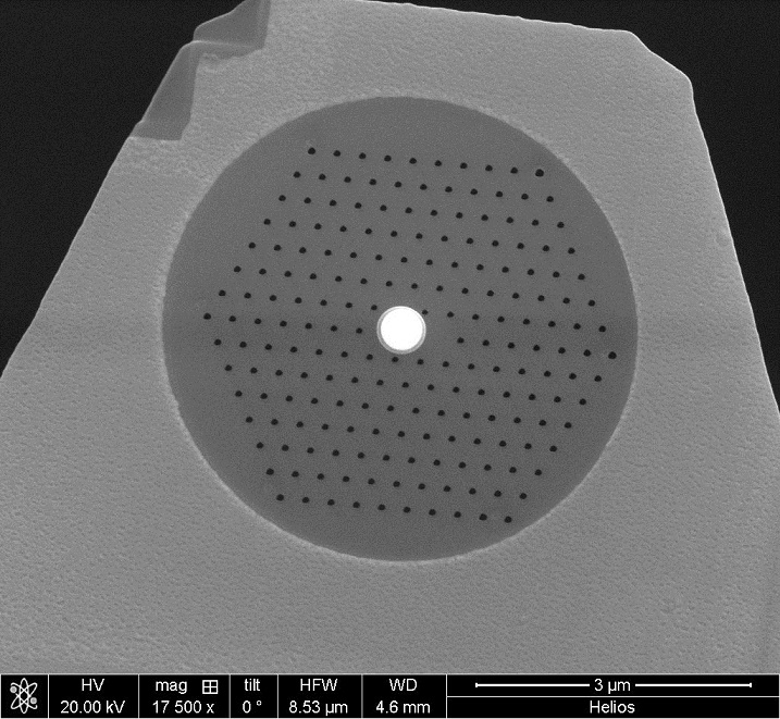
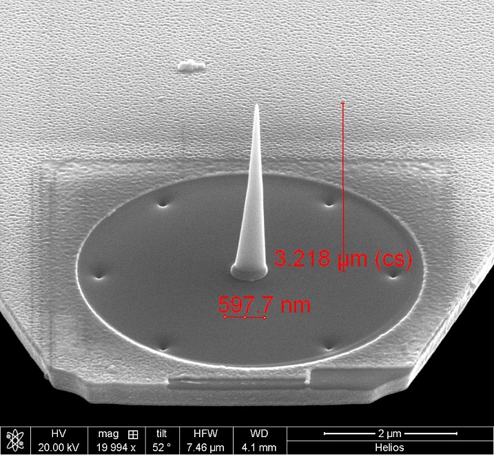
The pattern contains an hexagonal pattern with 196 holes with a distance of 275 nm between each other and nominal diameter of 45nm. We will not mill the whole cavity, but just the most external holes as markers. Moreover we need the whole pattern for measurement. Anyway, the proper settings for the ion column are V=30kV and I=24pA. So we stilt at 52° the chip, turn on the FIB column and work at the beginning on the cantilever A, the one that we will not use, in order to get a good focus and correct the ion column astigmatism. When the astigmatism is correct, we try to find the correct number of passes to pass through the cantilever without enlarging the holes too much. From previous measurements, it seems that 30 passes with a dwell time of 100 μs can be sufficient. When we obtain good holes, we move to the cantilever B, the one that we need. We will correct again the focus on the very end of the cantilever or at his base. Then we find a suitable position for the photonic crystal cavity. A good idea is to go near the end of the cantilever, but not too near the end. It is sufficient to be equally far from the three sides of the cantilever, like 1 μm distance.
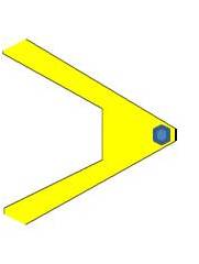
Then we mill the external holes of the hexagonal cavity, that is 6 markers. We check with the electronic column whether the holes pass through the cantilever and we go back at 0° for the cone deposition. The parameters used for the cone growth are V=20 kV and I=0.4 nA. It is important to put the cone in the exact center of the future cavity, so we have to increase the zoom to the smallest field of view that will show all the markers. We prepare the platinum deposition heating the source and we insert the GIS. We have to put the pattern of the cone centered in the zero position and, with the shift knobs, move the beam until we see that the markers are equally separated from the center. Then we can flow the gas, correct again the position and start the building of the cone. Remember that, once the gas is flowing, it will deposit quickly beyond the field of view, since the electronic current is quite high. But in this case is not a problem since we will clean the sample later. At this point the image of the cantilever should be like in the following figure.
As we can see, there is a wide darker area on the cantilever. That is the platinum deposited all around. It is important to remove it at least from the place where the photonic cavity will be, that is in the area between the markers and the cone. So we create a circular pattern, with outer diameter of 5 μm and inner diameter of 600 nm or less. In fact we have to cover all the area around the cone and until the markers, but also we don’t want to mill the cone away. So the inner diameter has to be big enough to keep the cone safe but small enough to remove all the platinum at the base. It is suggested to use a short dwell time for the circular crown, since we have to stop the milling when we have removed all the platinum. So we start the milling and we see in almost real time what happens. We will notice that the gold and the platinum will be removed much faster at the extremity of the pattern respect to the center. That is because the platinum deposition near the center was higher. When also near the cone the platinum has gone, we stop the milling. The result will be the following.
We can see that the base of the cone has a little bulge. It is important to decrease this bulge as much as possible since it will affect the plasmonic propagation. So we can reduce the inner diameter of the milling pattern or shift the ion column during the milling to remove the platinum near the cone. When we are satisfied, we can go back at 0° and remove the sample from the chamber. There’s another delicate part. We have to work on the opposite face of the cantilever, so, with extreme care, we have to detach the chip from the carbon tape and turn it upside-down. Then we have to attach it again on the carbon tape with the silicon nitride adhering. The correct way is to put the side with the cantilever under work protruding from the tape, otherwise the risk to attach and break the cantilever becomes very high. So, after the rotation, we insert the stub back in the chamber, we search for our cantilever and we tilt again at 52°. Again we can go to the cantilever A to correct the astigmatism, then back to the cantilever B for last focus correction. we can also focus and do some gold removal on the cantilever B, the important thing is to stay away from the part where we will put the photonic cavity. So, when we have a good quality of the beam, we have to search for the markers. On those markers we have to align the pattern for the plasmonic crystal. If the markers are not really clear, we can rely on another help, that is the platinum. In fact, during the cone growth, the gas fills the chamber. Since the electrons can travel deep into the substrate, they can also pass through it and catch the platinum gas at the other side, causing a deposition on the back of the cantilever. So it is possible to see the “shadow” of the cone on the back of the cantilever; this will help to align the pattern and avoid milling the cone. So, once the markers are in position, we mill the whole cavity, 196 holes. After that, again, we can remove all the traces of platinum using a full circle of around 5 μm diameter. The result is shown below.
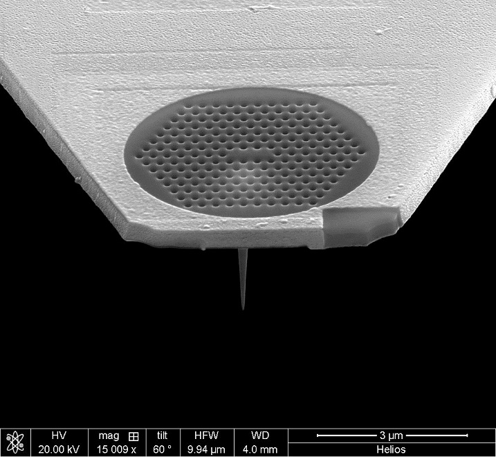
As we can see, the holes didn’t touch the cone bases, otherwise the cone will be bent. So, the structure is almost ready, now we have to distribute gold everywhere. So we remove the stub from the chamber and again, with great care, we attach the chip on the lateral side. We set 60 nm as final thickness in the spiedo mode to deposit 30 nm on both sides. When it’s finished, we turn the chip again with the glass adherent to the tape and we observe the final result with the electronic column. Here it is.