Gold Drifting
Move atoms were needed
Techniques to migrate gold atoms through annealing and nanostructures
Techniques to migrate gold atoms through annealing and nanostructures

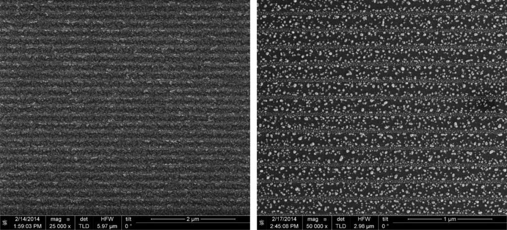
It is known that silicon and gold don’t bind very well, especially when the silicon is perfectly smooth and the gold is just a few nm thick. So, if the silicon substrate is annealed at high temperature (around 500°C), the gold atoms on it migrate on the surface until they find "accumulation points" and they start to nucleate, creating small spheres randomly distributed on the surface. Impurities and dirt can be an accumulation point for the gold. Below is an example of annealinng of a thin layer of gold at two different thickness and temperature.
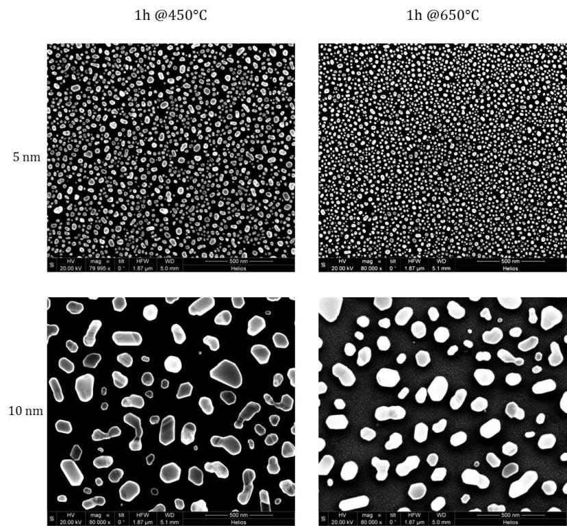
The higher the temperature, the more energetic will be the gold atoms, so they will travel further and will have more energy to escape from the defects of the silicon. This results in bigger gold aggregates. The higher the gold thickness, the bigger the aggregates and also the higher the probability to overfill the defects.
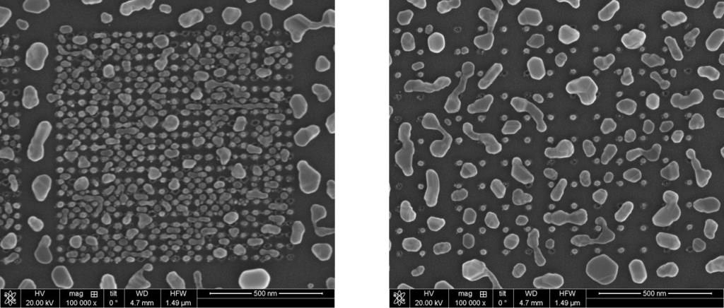
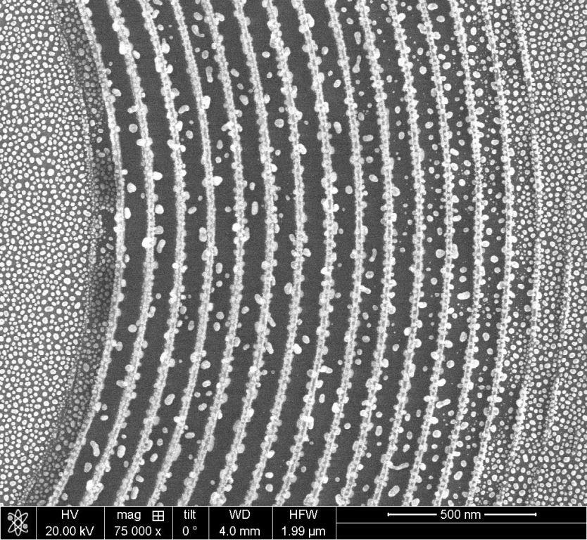
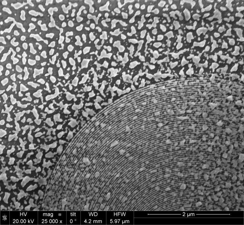
We want to observe how we can modify the drifting of the gold during the annealing. We want to introduce some nanostructuring on the silicon before the gold deposition. So we want to see, in the end, whether the nanostructuring provides a "direction" for the gold accumulation. The nanostructures can be lines of 10 to 50 nm milled with the FIB or also circles. As seen in the image above, gold forms points of accumulations more or less at a certain distance, around 100 nm for 10 nm thick layers, so it can be interesting to separate these structures more or less at the same amount
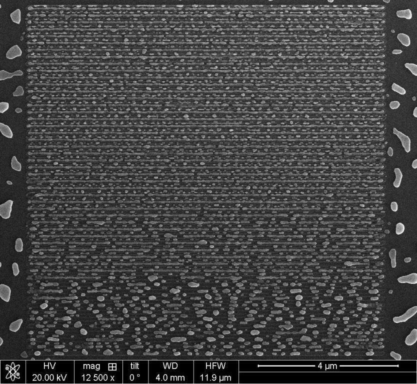
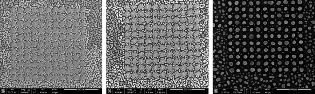
We fabricated patterns with the ion beam at low currents (1.1 or 7.7 pA) to avoid extensive damage around the patterned area. We defined two different set of patterns, lines and circles. divided in 4 areas. In the first area I drew some lines, with a distance of 50 nm and various depths from 100 nm to 20 nm (set on the FIB). I used an ion current of 1.1 pA and a dwell time alternating between 100 and 80 µs. The second frame was filled with lines distant 100 nm, written with a current of 7.7 pA and a dwell time of 1 µs. The third square had 150 nm distant lines and 200 nm distant lines, again at 7.7 pA. All the lines were done with a cross-section pattern, setting the y-pitch accordingly. In the fourth square I drew some circle with a pitch varying from 50 to 200 nm, current of 7.7 pA and dwell time from 10 µs to 100 µs. After the milling I cleaned the sample with acetone, IPA and water. I sputtered 10 nm of gold and I brought the sample to the an oven. I set a raising ramp of 5°C/minute, a set point of 500°C and a decreasing ramp of 3°C/minute. The temperature was kept at the set-point for 1 hour. Below is the result.
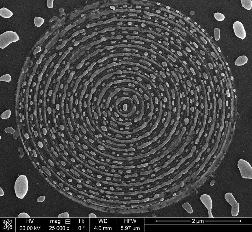
The best outcome was seen with the structures separated by 200 nm. As seen in the image above, we could almost obtain contiguous distribution in the circles. Instead, on the figure below, we can appreciate that the depper the lines, the higher is the possibility to create continuous segments of gold. In fact the gol atoms cannot exit from the trenches, so they act as accumulating points for the nearby atoms.
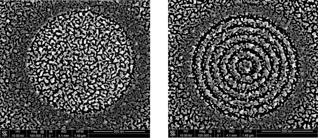
We tried also with milled dots, with a pitch from 40 to 100 nm and diameters of 15 nm. We wanted to accumulate gold atoms only in the holes and not around. Also in this case, the deeper the milling, the higher the chance of creating successful accumulation. Below is an image of annealing at 500°C of a 10 nm thick layer of gold in dots with a pitch of 50 (left) and 100 nm (right).
We tried to create defects not only by milling but also with electron beam-iduced deposition (EBID) of platinum-carbonium. As in the FIB milling, we patterned lines, circles and dots of platinum to act as aggregation features. We also reduced the layer of gold down to 3 nm to appreciate a better migration of the atoms. For the circles, we used again different pitch and dwell time. The annealing temperature was decreased to 200° C. In the image below we can see the migration of atoms over a full platinum circle (left) and on circular lines of platinum (right). As we see, in the first case there is not much difference between the inside and outside of the platiunum area, however on the right image, the gold follows pretty well the platinum patterns.
Then we tried deposting platinum in a sqaured array of points. again we deposited 3 nm of gold and we observed the annealing at increasing temperature. As shown in the figure below, increasing the temperature the gold atoms accumulate more around the platinum dots.
We wanted to explore the migration of gold around polymeric structures. At first we tried with Poly(methyl methacrylate) (PMMA) A2 diluted 2:1 in Anisole. We created patterns with different shapes, rings and parallel lines exposing at 20 KeV and 25 pA at the EBL. We noticed a different migration pattern on the polymer respect to the unexposed area, but we didn't notice a good aggregation.
Increasing the temperature, the gold just forms small aggregates along the polymer, it seems that the polymer limits the migration too much.
We tried another polymer, Hydrogen silsesquioxane (HSQ), a high resolution polymer diluted 6% in Methyl isobutyl ketone (MIBK). Spinning the resist at 5000 rpm we obtained walls 100 nm high and 20 nm thick. These walls were too high, but we obtained some good results as shown below.
We diluted the HSQ at 1% in MIBK, obtaining lines 30 nm tall but the results didn't improve.
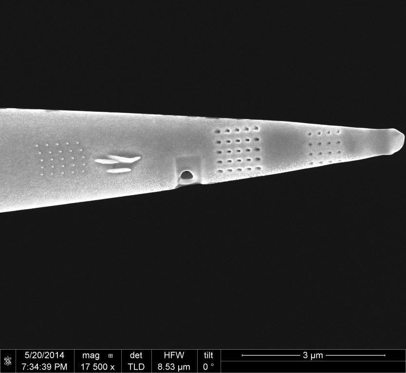
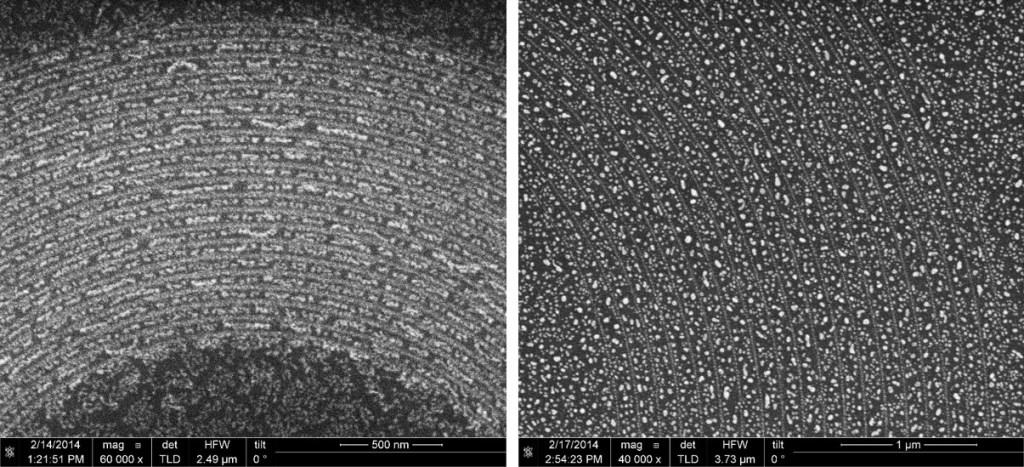
Managing the migration of gold atoms can lead to interesting application. A promising idea is to deposit patterned gold on surfaces that are not easily spinned, like tapered fibers and rods. So we took optical and snom fibers, we cut one head and we produced some dot array on the tip, to show the gold aggregations. Moreover we can show that, provided that the fiber works in the visible, like at 532 nm, it is possible to do Raman spectroscopy in a dense, turbid environment.
In this case the fabrication is quite challenging because the fiber accumulates a lot of charges, making very difficult to create good holes. From the previous tests I saw that 200°C is not enough to appreciate a good movement of the gold, so I have to try at least 300°C. In any case, temperatures superior to 400°C make the fiber extremely rigid and thus fragile, probably they consume the external polymer capsule and so the fiber lose elasticity. Same issue with the capillaries, but here the annealing temperature has to be even lower because of the insertion part that stands up to 250°C. Also, if the analysis pre-annealing is tasky, the post-annealing imaging is even worse, due to the movement of gold that creates even more accumulation of charges on the SiO substrate. Sometimes we can see the reflection of the vacuum chamber.
Anyway, first we tried with optical fibers, creating patterns with FIB milling as in the silicon substrate. We could appreciate an interesting result with an annealing of 200°C, while increasing the temperature worsen the distribution.
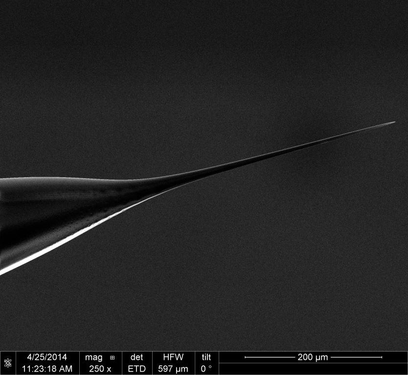
Then we used femtotips, tapered capillaries with a tip down to 50 nm.
We created some patterns on the side, either holes or platinum dots, to observe the gold migration at different annealing temperatures. Unfortunately we didn't achieve good results yet.